Excellent video on PCB stack-up and other issues:
")
Notes:
- decoupling caps between power ground planes help if a traces changes from ground reference to power, but this only works up to 200-300MHz. (This would be typical of 4-layer board with signal, gnd, power, signal)
- keep power and ground planes close to each other < 0.2mm (8mil), then the planes look like a capacitor.
- power plane reference should be the same power source that generated the signal
- very small amounts of energy can cause EMI problems, where much higher amounts of energy are required to cause signal integrity problems.
- energy couples by the square of the distance
- to couple planes, place via every 10th wavelength of highest frequency
- inductance between power planes must be low
- its not our job to make things easy, its our job to make them work
- pouring ground on top/bottom layers lowers EMI not because it is a shield, but because it is a reference for signals and power
- there is no 4-layer stack-up that is wonderful
- vias have highest inductance of anything in the board stackup
- keep power and ground near surface because power delivery needs low inductance
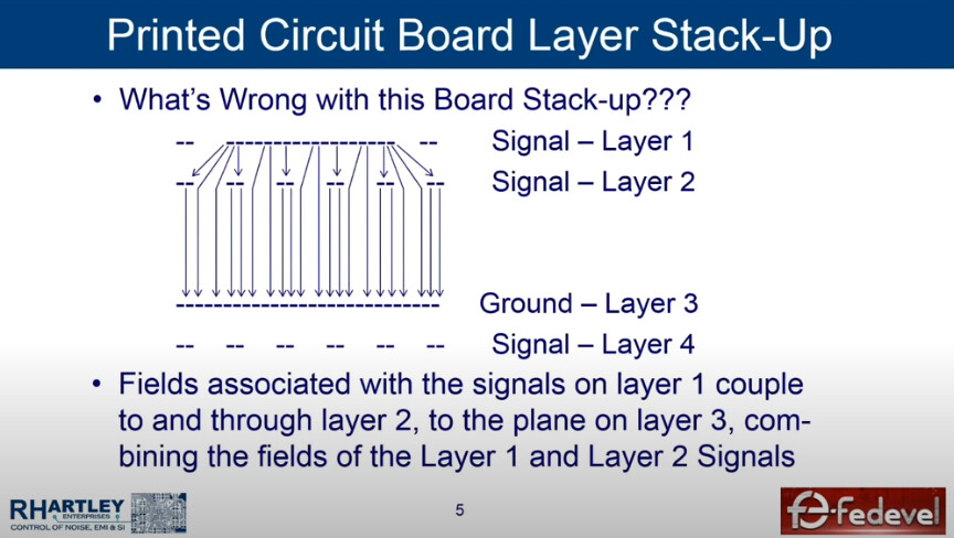
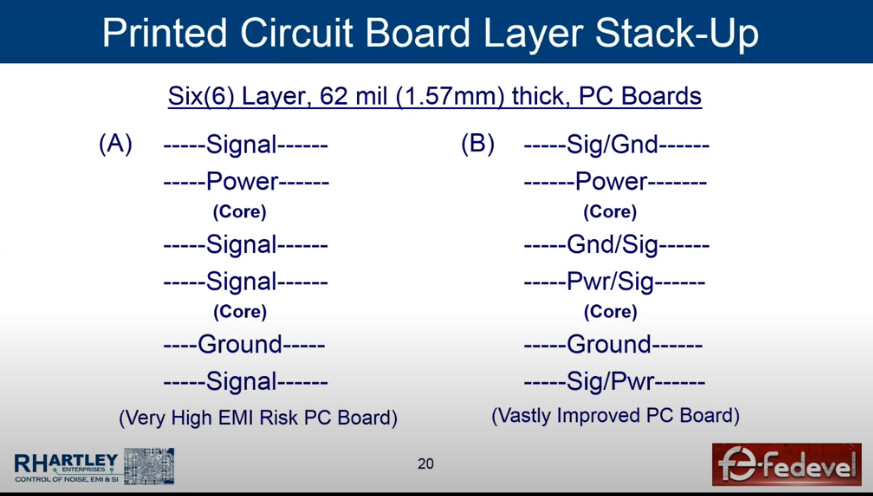
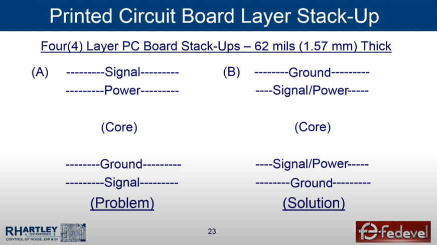
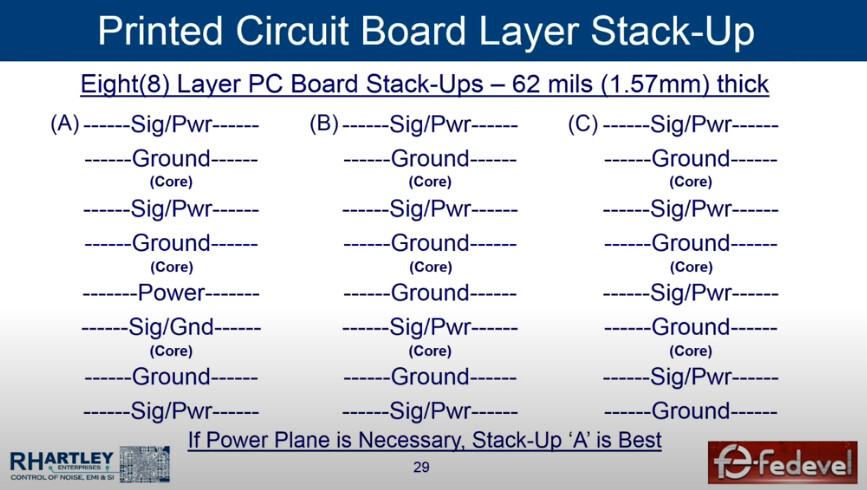
A few screenshots:
In the below board, the change from a classical 4-layer stackup (A) to (B) improve EMI performance because it improved the cap coupling between ground and power.

")